搬运以前写在别的地方的文章
单核
首先查阅wiki(zh.m.wikipedia.org/zh-hans/比较并… ,注意到以下句子。
实现CAS操作基于CPU提供的原子操作指令实现。对于Intel X86处理器,可通过在汇编指令前增加LOCK前缀来锁定系统总线,使系统总线在汇编指令执行时无法访问相应的内存地址。而各个编译器根据 这个特点实现了各自的原子操作函数。
由此猜测cas是一条汇编指令,搜索得到《cpu cmpxchg指令理解(CAS)》。
知道了指令就好办了,谷歌搜索“ia32 instruction set manual”,得到指令集文档。
www.intel.com/content/dam… www.intel.com/content/dam…
在3-2章节中找到CMGXCHG和CMPXCHG8B/CMPXCHG16B,关键内容如下:

Description Compares the value in the AL, AX, EAX, or RAX register with the first operand (destination operand). If the two values are equal, the second operand (source operand) is loaded into the destination operand. Otherwise, the destination operand is loaded into the AL, AX, EAX or RAX register. RAX register is available only in 64-bit mode.
This instruction can be used with a LOCK prefix to allow the instruction to be executed atomically. To simplify the interface to the processor’s bus, the destination operand receives a write cycle without regard to the result of the comparison. The destination operand is written back if the comparison fails; otherwise, the source operand is written into the destination. (The processor never produces a locked read without also producing a locked write.)
In 64-bit mode, the instruction’s default operation size is 32 bits. Use of the REX.R prefix permits access to additional registers (R8-R15). Use of the REX.W prefix promotes operation to 64 bits. See the summary chart at the beginning of this section for encoding data and limits
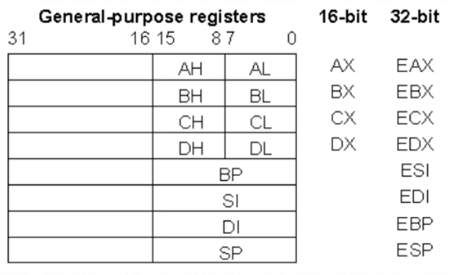
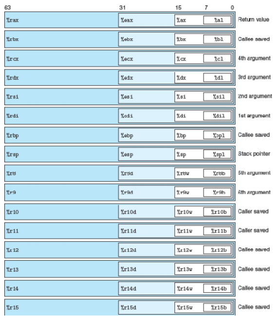
顺带一提: AL,AX,EAX,RAX其实是同一个寄存器


多核
前面写的文档,其实只解决了单核上的cas问题,那么多核上的cas是如何处理的呢?
我们可以继续查阅 www.intel.com/content/dam…
可以看到
This instruction can be used with a LOCK prefix to allow the instruction to be executed atomically. To simplify the interface to the processor’s bus, the destination operand receives a write cycle without regard to the result of the comparison. The destination operand is written back if the comparison fails; otherwise, the source operand is written into the destination. (The processor never produces a locked read without also producing a locked write.)
那么继续查阅LOCK的文档,可以看到
Description
Causes the processor’s LOCK# signal to be asserted during execution of the accompanying instruction (turns the instruction into an atomic instruction). In a multiprocessor environment, the LOCK# signal ensures that the processor has exclusive use of any shared memory while the signal is asserted.
In most IA-32 and all Intel 64 processors, locking may occur without the LOCK# signal being asserted. See the “IA-32 Architecture Compatibility” section below for more details.
The LOCK prefix can be prepended only to the following instructions and only to those forms of the instructions where the destination operand is a memory operand: ADD, ADC, AND, BTC, BTR, BTS, CMPXCHG, CMPXCH8B, CMPXCHG16B, DEC, INC, NEG, NOT, OR, SBB, SUB, XOR, XADD, and XCHG. If the LOCK prefix is used with one of these instructions and the source operand is a memory operand, an undefined opcode exception (#UD) may be generated. An undefined opcode exception will also be generated if the LOCK prefix is used with any instruction not in the above list. The XCHG instruction always asserts the LOCK# signal regardless of the presence or absence of the LOCK prefix.
The LOCK prefix is typically used with the BTS instruction to perform a read-modify-write operation on a memory location in shared memory environment. The integrity of the LOCK prefix is not affected by the alignment of the memory field. Memory locking is observed for arbitrarily misaligned fields. This instruction’s operation is the same in non-64-bit modes and 64-bit mode. IA-32 Architecture Compatibility Beginning with the P6 family processors, when the LOCK prefix is prefixed to an instruction and the memory area being accessed is cached internally in the processor, the LOCK# signal is generally not asserted. Instead, only the processor’s cache is locked. Here, the processor’s cache coherency mechanism ensures that the operation is carried out atomically with regards to memory. See “Effects of a Locked Operation on Internal Processor Caches” in Chapter 8 of Intel® 64 and IA-32 Architectures Software Developer’s Manual, Volume 3A, the for more information on locking of caches.
下载
www.intel.cn/content/www… www.intel.cn/content/www… 可以看到:
For the Intel486 and Pentium processors, the LOCK# signal is always asserted on the bus during a LOCK operation, even if the area of memory being locked is cached in the processor. For the P6 and more recent processor families, if the area of memory being locked during a LOCK operation is cached in the processor that is performing the LOCK operation as write-back memory and is completely contained in a cache line, the processor may not assert the LOCK# signal on the bus. Instead, it will modify the memory location internally and allow it’s cache coherency mechanism to ensure that the operation is carried out atomically. This operation is called “cache locking.” The cache coherency mechanism automatically prevents two or more processors that have cached the same area of memory from simultaneously modifying data in that area.
至此,cas在多核上的疑惑也解开了。