

The Intel 4004 after 44 years! 2015 Progress Report
A new foundation for the future: teaching young and old about microprocessor basics
Tim McNerney's original goal for starting this project was to make the invisible machinery of the first computers-on-a-chip visible and understandable to students and the lay public. The 4004 is great for many reasons, but for this project it's number one selling point is that it is a minimal CPU. This is extremely useful for teaching purposes. In the coming months before the 45th anniversary, we will be working to make the 4004 and fundamentals of computers and digital logic even more accessible though the confluence of art, education, and technology. This project could never have been done alone. It needed an international team of volunteers.
New: Scalable Vector Mask Artwork for Museum-sized Exhibits
For years, our project made do with mask artwork scanned from an Intel Archives' set of aging mask proof transparencies. These were invaluable for making silkscreens for the Intel Museum exhibit's 16x23 inch "big chip" 4004 replica still on display. Later, with some bitmap scaling, alignment, and careful corrections, thanks to Lajos Kintli, we succeeded in verifying them against Fred Huettig's paintstakingly re-captured schematics.
If you look too closely, the old proof set artwork is pretty ugly, certainly nothing we could use if we wanted to build a larger museum exhibit, say 3x4 feet, or import the mask artwork into a PCB layout package to build a giant, working circuit board. The old artwork just wasn't going to cut it. So McNerney took a pair of high-resolution photomicrographs (kindly donated by reverse engineer extraordinaire, Christopher Tarnovski), and set out to trace every wire, transistor, resistor, and capacitor using Adobe Illustrator. Just hours before the 44th anniversary, he finished tracing the first, complete draft of the mask set artwork. The next step is to verify it against the schematics and try it out in simulation. (As of 11/15/15 there were undoubtedly a few errors to fix, but we already have verification software ready to use for catching and fixing the inevitable little mistakes.)
The complete chip: A composite of the mask artwork—six layers in all: metal, polysilicon, diffusion, vias, buried contacts, and passivation.
查看图片Detail of the DRAM decoders and "4004" label.
查看图片Celebrating the unsung artists of Silicon Valley: Rubylith cutters
Back in the early 1970s, there was no electrical CAD software, design-rule checkers were people, and Adobe was still just the name of the little creekbed that ran through my back yard in Los Altos, California. VLSI "artwork" was hand-crafted on giant light tables by "rubylith cutters." Semiconductor engineers like Federico Faggin would draw parts of the layout on paper, trying to squeeze as much digital logic into a 3x4 millimeter rectange of silicon as they could. The rubylith cutters turned engineering sketches into the carefully aligned, lithographic masks that would be photo-reduced and used to fabricate (mass produce) the actual semiconductor chips.
If you know any of these unsung heros, or were one yourself, please contact us. We'd love to hear your stories.
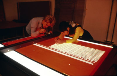
(Photo courtesy of Intel, as published on the Computer History Museum web site)
This is is an "X-ray" composite of two photomicrographs we used to re-create the mask artwork: one with metal stripped away, exposing the partially hidden polysilicon, diffusion, and buried contact layers. The original, unstripped die photo, is "ghost" superimposed, making the metal layer appear see-through, while still revealing the underlying detail.
Revision 2 of the 2010 Busicom 141-PF replica PCB
Bill Kotaska "beat us to the punch" with the replica he built in 2008, complete with a printer salvaged from another vintage calculator. But still, in 2010, we wanted to make a PCB based replica of our own using vintage chips: the original 4002s, 4003s, and 4004, plus a 4201 clock generator, and a 4289 memory interface (so we could use an old EPROM to replace the impossible-to-find, custom-programmed 4001s with the Busicom firmware... yes, not even on eBay). Now we are working on Revision 2, with corrections and improvements.
Here is the first version that I designed, fabricated, and assembled. Not quite working before my visit to Hungary in 2010, I still I brought the prototype to Lajos Kintli as a gift, and with a handful of corrections and new printer emulator firmware, he got it working (see printer output below).
查看图片Shinshu-Seiki Model 102 printer emulator code
Lajos Kintli's printer emulator for the PIC18F2585 converts the hammer signals to serial. This lets you view printer output from the replica on a PC terminal window (as shown below) or on real hardware using a small LCD panel with a serial input. The printer emulator is also important simply to make the Busicom calculator software work at all, by providing a "heartbeat" signal that was generated by the spinning printer drum in the original.
查看图片Credits
- Fred Huettig, schematic capture, museum electronics, FPGA design
- Lajos Kintli, verification software, reverse engineering: software, 4001
- Christopher Tarnovski, high-resolution die photographs of 4004
- Brian Silverman, simulation software, strategy
- Barry Silverman, simulation software
- Tom Knight, die photographs of 4001
- Federico Faggin, in many ways, including 4001 prototypes
- Computer History Museum, contents of 4001 Busicom ROMs
- Tracey Mazur, Intel, funding, located 4004 schematics, mask proofs
Legal Notices
- The software (e.g. simulators) and engineering documents (e.g. schematics, drawings, etc.) are provided "AS IS" with no warranty expressed or implied. Fitness for any particular purpose is not guaranteed. The authors do not accept any liability for use of this information.
- The works on this web site are licensed under a Creative Commons Attribution-Noncommercial-Share Alike 2.5 License.
